Antipyretics for children are prescribed by a pediatrician. But there are situations of emergency care for fever, when the child needs to give the medicine immediately. Then the parents take responsibility and apply antipyretic drugs. What is allowed to give to infants? How can you bring down the temperature in older children? Which medications are the safest?
A semiconductor diode is an electroconversion semiconductor device with one rectifying electrical transition having two terminals.
A semiconductor diode is a semiconductor device with one electrical transition and two leads (electrodes). Unlike other types of diodes, the principle of operation of a semiconductor diode is based on phenomenon p-ntransition.
The diode (from other Greek, δις - two and -one of the signifying path) - a two-electrode electronic device, has a different conductivity depending on the direction electric current. The diode electrode connected to the positive pole of the current source when the diode is open (i.e., has a small resistance) is called anode, connected to the negative pole - cathode.
The current in the chain of the lamp anode depends on the filament temperature, that is, on the amount electrons , emitted from the cathode in a unit of time, as well as from the voltage at the anode. If the positive voltage at the anode is small, it attracts a small number of electrons and the current in the anode circuit is small. With increasing voltage at the anode, the current in the circuit increases.
Fig. 2.2. Diagram of the structure of a semiconductor diode (a) and its graphic designation (b)
The letters p and n denote semiconductor layers with p-type and n-type conductivities, respectively. In the contacting layers of the semiconductor (the region of the p-n junction in Figure 2.2), diffusion of holes from layer p to layer n takes place, the reason of which is that their concentration in layer p is much larger than their concentration in layer n. As a result, in the border regions of layer p and layer n, there is a so-called depletion layer, in which the concentration of mobile charge carriers (electrons and holes) is small. The depleted layer has a large resistivity. The ions of impurities of the depleted layer are not compensated by holes or electrons.
Together, the ions form uncompensated volumetric charges creating an electric field with a strength of E. This field prevents the passage of holes from layer p to layer n and the transition of electrons from layer n to layer p. It creates a so-called drift flow of mobile charge carriers that moves holes from layer n to layer p and electrons from layer p to layer n. Thus, depending on the polarity of the current passing through the diode, the conductivity of the diode changes significantly, leading to a change in the magnitude of the passing current.
A diode is an electronic device with a pronounced one-sided conductivity of an electric current: it flows well through itself a current in one direction and very badly in the other. This basic property of a diode will in particular be used for conversion alternating current electric lighting network into a constant current necessary for powering electronic control devices. A schematic device and a conditional graphic designation of a semiconductor diode are shown in the figure.

It is a small plate of germanium or silicon, one region (part of the volume) of which has a p-type electrical conductivity, that is, a "hole", the other - an electrical conductivity of the n-type, that is, the electron. The boundary between them is called the p-n junction. Here the letters p and n are the first in the Latin words positiv - "positive", and negativ - "negative". The p-type region of the source semiconductor of such a device is an anode (positive electrode), and the n-type region is a cathode (negative electrode) of the diode.
The principle of operation of the diode is illustrated by the diagrams shown in the figure.
![]()
If the battery GB is connected to the diode VD through the incandescent lamp HL so that the positive pole terminal of the battery is connected to the anode, and the negative pole terminal to the diode cathode a), then a current appears in the formed electrical circuit, which will be signaled by the HL lamp that is lit. The maximum value of this current depends on the resistance of the p-n junction of the diode and the DC voltage applied to it. Such a state of the diode is called open, the current flowing through it is a direct current I pr, and the voltage applied to it, due to which the diode was in the open state, is a direct voltage Upr.
If the poles of the GB battery are interchanged, as shown in Fig. b, the HL lamp does not light up, since in this case the diode is in the closed state and renders a large resistance to the current in the circuit. A small current through the p-n junction of the diode in the opposite direction will still go, but in comparison with the direct current will be so insignificant that the lamp filament does not even react. This current is called the reverse current I ob, and the voltage creating it is the reverse voltage U of the sample.
Main characteristics and parameters of diodes:
Frequency range of the diode;
Breakdown voltage.
Semiconductor diodes have the following main settings:
Permanent reverse diode current (I ob) - value direct current, flowing through the diode in the opposite direction at a given reverse voltage;
The constant reverse diode voltage (U ob) is the value of the DC voltage applied to the diode in the opposite direction;
The constant forward current of the diode (I pr) is the value of the direct current flowing through the diode in the forward direction;
The constant direct voltage of the diode (U pr) is the value of the direct voltage on the diode for a given constant direct current;
The limiting mode of operation of diodes is characterized by maximum permissible parameters - parameters that provide a given reliability and whose values should not be exceeded under any operating conditions:
Maximum permissible power dissipation (P max);
The maximum permissible constant forward current (I pr max), the value of which is limited by the heating of the pn junction;
The maximum permissible constant reverse voltage (U out of max);
Differential resistance (r diff);
The minimum (T min) and the maximum (T max) of the ambient temperature for the operation of the diode.
The permissible dissipated power (P mах) is determined by the thermal resistance of the diode (R m), the permissible transition temperature (Т п mах) and the ambient temperature (Т о) in accordance with the relation:

The maximum permissible forward current can be determined from the specified maximum permissible power:

The inverse maximum permissible voltage (U out of max) for different types of diodes can take values from several units to tens of thousands of volts.
It is limited by the breakdown voltage:
U ob max? 0,8 U samples.
The differential resistance (r diff) is equal to the ratio of the voltage increment on the diode to the small increment of current through the diode that caused it:
Resistance r diff depends on the mode of operation of the diode.
The minimum ambient temperature (T min) at which semiconductor diodes can be used is usually -60 ° C. At lower temperatures, electrical and mechanical properties of semiconductor crystals and elements of diode structures deteriorate.
For germanium diodes, the maximum temperature T max = +70 ° C. For flint crystals, it can reach +150 ° C. At higher temperatures, the semiconductor degenerates: the concentrations of the main and minority carriers become identical, the transition ceases to possess the properties of one-sided conductivity
The current-voltage characteristic is the dependence of the current i flowing through the diode on the voltage u applied to the diode. The current-voltage curve is also called the current-voltage characteristic (Figure 2.3).

A model analogue of a barrier capacitance is the capacity flat capacitor, the plates of which are r-and nregion, and the dielectric serves pn-transition, which has practically no moving charges. The value of the barrier capacity varies from tens to hundreds of picofarads; The change in this capacitance with a voltage change can reach tenfold.
Diffusion capacity.The change in the magnitude of the space charge of nonequilibrium electrons and holes, caused by a change in forward current, can be considered as a consequence of the presence of a so-called diffusion capacity, which is connected in parallel with the barrier capacitance.
The values of the diffusion capacity can range from hundreds to thousands of picofarads. Therefore, for direct voltage, the capacitance pn-transition is determined mainly by diffusion capacity, and at reverse voltage - by barrier capacitance.
The diodes are usually characterized by the following parameters (Figure 2.3):
The reverse current for a certain value of the reverse voltage I ob, μA;
Voltage drop on the diode at a certain value of the forward current through the diode Upr, V;
The capacitance of a diode when a reverse voltage is applied to it of a certain value of C, pF;
Frequency range in which operation is possible without reducing the rectified current fgp, kHz;
Diodes of different types differ in their parameters and characteristics. The main parameters of the diode are: the filament voltage U, the filament current I n, the emission current Ie, the anode voltage Ua. In addition, the diodes differ in the steepness of their characteristics. The faster the anode current of the diode rises as the anode voltage increases, the greater the slope of the diode characteristic. The steepness is denoted by S It shows how many milliamps the anode current of the diode increases as the anode voltage rises by 1 V:
where? Ia- is the change in the strength of the anode current,
Ua is the change in the anode voltage.
So, if the slope of the diode is S -3 mA / V, then this means that when the anode voltage is increased by 1 V, the anode current increases by 3 mA.
The parameters that characterize the diode are also the magnitude of its internal resistance to alternating current. The internal resistance of the diode is not constant, but depends on the magnitude and polarity of the anode voltage applied to the diode. For example, when a negative voltage is applied to the anode, its internal resistance is practically infinitely large and the current does not pass through the diode.
The diode has the smallest internal resistance within the limits of the average rectilinear part of the Characteristics, where the steepness has the greatest value. At the bottom of the characteristic and at the top, the internal resistance of the lamp increases.
The internal resistance of the lamp is denoted by H ;. It is equal to the ratio of the change in the anode voltage (Ua) to the corresponding change in the anode current:
A very important parameter characterizing each lamp is the permissible power of the scattering at the anode. Electrons under the influence of the voltage applied to the anode, develop a high speed and therefore with a significant force hit it. At the same time, the anode, heated, can become hot and even melt. The higher the anode voltage, the greater the velocity of the electrons. The more current passing through the diode, the greater the number of electrons simultaneously striking the anode. Therefore, the amount of heat released at the anode depends on the anode voltage and the anode current. The product of these two quantities is equal to the power dissipation at the anode:
Heat release at the anode is a useless, but inevitable loss of power. With a very strong heating of the anode, the lamp fails. In view of this, the scattering power should not exceed a certain value for a given type of lamp.
The technical conditions usually specify the maximum (or minimum) parameter values for diodes of each type. For example, the maximum possible value of the reverse current, direct voltage drop and diode capacitance is set. The frequency range is set by the minimum value of the boundary frequency fgp. This means that the parameters of all the diodes do not exceed (and in the case of a frequency - not lower than) the specified technical conditions values.
The designation of diodes consists of six symbols:
The first symbol (letter or number) denotes the diode material (the number denotes diodes capable of withstanding a higher temperature):
G or 1 - germanium;
K or 2 - silicon;
A or 3 - gallium compounds;
The second symbol (letter) indicates the subclass of instruments:
A - super-high frequency; B - with a volumetric the Gunn effect ; AT - varicaps ; Г - noise generators; D - rectifying, universal, pulsed; And - tunnel and inverted; K - current stabilizers; A - radiating; H - dinistors ; C - zener diode stabilizers; U - thyristors ; C - rectifying poles and blocks;
The third symbol (number) denotes the classification number by which the diodes inside this type are distinguished (for example: 1 - low power, 2 - medium power, 3 - high power, 4 - universal, etc.).
The fourth and fifth symbols (numbers) indicate the development serial number (from 1 to 99).
The sixth character (letter) indicates the difference in parameters that are not classification.
Classification and notation. Classification of modern semiconductor diodes (PD) by their purpose, physical properties, basic electrical parameters, structural and technological characteristics, the initial semiconductor material is reflected in the system of symbols of diodes in accordance with GOST 20859.1-89.
The first element (number or letter) denotes the initial semiconductor material, the second (letter) is a subclass of instruments, the third (figure) is the basic functionality of the device, the fourth is the number designating the development serial number; the fifth element is the letter conventionally defining the classification (sorting by parameters) of devices manufactured using a single technology.
The following symbols are used to indicate the initial semiconductor material:
G, or 1 - germanium or its compounds; K, or 2 - silicon or its compounds; A, or 3 - gallium compounds; And, or 4 - indium compounds.
To denote subclasses of diodes one of the following letters is used:
D - rectifier and pulse diodes; C - rectifying poles and blocks; B - varicaps; And - tunnel diodes; A - superhigh-frequency diodes; C - zener diodes; Г - noise generators; A - emitting optoelectronic devices; O - optocouplers.
There are diodes:
depending on the purpose :
Straightening; zener diodes;varicaps; tunneling; impulse and others;
on the raw materials used :
Germanium; silicon; from gallium arsenide;
on manufacturing technology :
Alloy; diffusion; planar;
by frequency range:
Low-frequency; high-frequency; Microwave diodes (superhigh-frequency diodes);
by the type of the pn junction :
Planar; point.
Zener diodes are silicon planar diodes designed to stabilize the level of the DC voltage in the circuit with a change in some limits of current through the diode. This is a semiconductor diode designed to work in the mode of electric breakdown. As noted in Sec. 1.2, if the reverse voltage exceeds the value U arr. etc , then avalanche breakdown occurs r-ntransition at which the reverse current rises sharply at an almost constant reverse voltage. Such a section of the characteristic (section ab, see Figure 1.8, a) use zener diodes, the normal inclusion of which in the circuit of the source of constant voltage is the opposite (see Figure 1.8, b).
If the reverse current through the zener diode does not exceed a certain value I Art. Max, the state of electrical breakdown does not lead to damage to the diode and can be reproduced for tens and hundreds of thousands of hours. Silicon is used as a starting material in the production of zener diodes, since the reverse currents of silicon r-ntransitions are small, and consequently, there are no conditions for self-heating of the semiconductor and thermal breakdown r-ntransition.
Basic parameters of the zener diode:
- rated voltage of stabilization U st nom - voltage on the zener diode in the operating mode (for a given stabilization current);
- minimum stabilizing current I st.min - the lowest value of the stabilization current, at which the breakdown regime is stable;
- the maximum allowable current stabilization I st.max — the maximum stabilizing current at which the heating of the zener diode does not exceed the permissible limits.
Differential resistance г ст - the ratio of the increase in the stabilization voltage to the increment of the stabilizing current causing it: g st =DU st/ DIAST.
The parameters of the zener diodes are also maximum allowable forward current I max , maximum allowable impulse current I pr.i max , maximum permissible power dissipation R max .
(ТКН) is the temperature coefficient of the stabilization voltage.
The level of the stabilization voltage is determined by the value of the breakdown voltage U arr. etc , which, in turn, depends on the width r-ntransition, and, consequently, the degree of doping of the silicon with an impurity. To obtain low-voltage stabilitrons, heavily doped silicon is used. Therefore, for zener diodes with stabilized voltage<5,4 В участок стабилизации определяется обратным током туннельного характера. У низковольтных стабилитронов с ростом температуры напряжение стабилизации уменьшается, а у высоковольтных увеличивается.
The circuit in Fig. 1.8, b explains the principle of operation of the simplest constant-voltage regulator. Increase in input voltage u in leads to an increase in current through the zener diode and resistance R. Excess input voltage is allocated to R, and the tension u out remains almost unchanged.
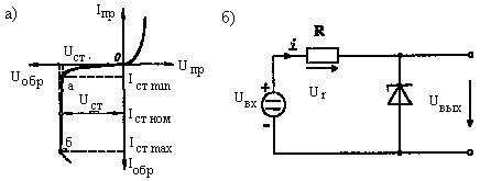
Fig. 1.8 Volt-ampere characteristic (a) and zener diode connection circuit (b)
In zener diodes, tunneling, avalanche, and mixed breakdown can occur, depending on the resistivity of the base.
Stabistor. It is a semiconductor diode, the voltage at which direct inclusion (about 0.7 V) depends little on the current (the straight branch in the corresponding section is almost vertical). Stabilist is designed to stabilize small voltages.
Varicap called a specially designed semiconductor diode, used as a capacitor of variable capacity. The value of the varicap capacity is determined by its capacitance r-ntransition and changes when the voltage applied to the transition (diode) changes.
As was said above (see Chapter 1.2), a direct r-n-transition is characterized, in particular, by diffusion capacity, and inversely - by barrier. Varicaps use a barrier capacitance (expression 1.12), characterized by a small temperature coefficient, a low level of intrinsic noise and a weak frequency dependence. Consequently, in the operating mode,
the varicap is subjected to a locking external voltage. Because the thickness p-nThe transition depends on the magnitude of the applied external voltage U, then, by changing the latter, it is possible to adjust the value of the capacity. This is used, in particular, for tuning to the desired channel in TVs and radios.
The main parameters of varicap are:
1. The total capacitance of the varicap Sv is the capacitance, measured at a certain reverse voltage (measured at U = 5V and is tens - hundreds of rF);
2. Coefficient of overlapping in capacity Кп = С in max / С in min - the ratio of the varicap capacitance at the two extreme values of the reverse voltage ( To n = 5-8 time);
3. Quality varicap Q = X c / r n Where X c- the reactance of the varicape; r n - resistance of active losses;
4. I arr - a direct current flowing through the varicap in the opposite direction at a given reverse voltage.
Varicaps are widely used for the electronic tuning of the resonant frequency of oscillatory circuits. By changing the voltage on the varicap connected to the oscillatory circuit, it is possible to provide remote and inertial control of the resonant frequency of the circuit. Thus, for example, to obtain the necessary intermediate frequency values, a smooth change in frequency must be provided in the heterodyne of the television receiver.
In TVs of old types, this setting is manually adjusted by the capacitor capacitance entering the oscillator circuit of the local oscillator, and in modern televisions this is done using a varicap included in the oscillator circuit of the local oscillator. When the voltage applied to the varicap varies, its capacitance changes, and, consequently, the heterodyne frequency. Variation of the voltage on the varicap can be carried out either manually (by a potentiometer) or by means of the LO system.
The tunnel diode is a semiconductor diode in which the phenomenon of tunnel breakdown is used when switched on in the forward direction. A characteristic feature of the tunnel diode is the presence on the straight branch of the current-voltage characteristic of a section with a negative differential resistance.
For example, in Fig. 1.12 shows a direct branch of the current-voltage characteristic of a germanium tunnel amplification diode 1I104A ( I pr.max = 1 mA - constant direct current, U mod.max = 20 mV), designed to amplify in the wavelength range 2-10 cm (this corresponds to a frequency of more than 1 GHz).
 Fig. 1.12 I-VAC of a tunnel diode
The total capacity of the diode at the minimum characteristic point is 0.8-1.9 pF. Tunnel diodes can operate at very high frequencies - more than 1 GHz. The presence of a section with a negative differential resistance on the current-voltage characteristic makes it possible to use tunnel diodes as an amplifying element and as the main element of the generators. At present, tunnel diodes are used precisely in this capacity in the region of ultrahigh frequencies.
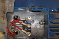
Rectifier diodes are intended for rectification of alternating current of low frequency (50-100 000 Hz). At present, silicon rectifying diodes with r-n-transition of planar type, having many times smaller reverse currents and large reverse voltages in comparison with germanium ones.
The main element of the rectifier diode is a semiconductor plate in which, by the fusion or diffusion method, r-n-transition. Silicic r-ntransition is formed by fusing the initial n-type silicon crystal with boron or aluminum. To protect against external influences, as well as to ensure good heat dissipation, a semiconductor plate with r-n-transition and two external leads from the layers p and n is the body
Rectifier diodes are divided into small ( I pr avg < 0,3 А), средней (0,3 А < I pr avg < 10 А) и большой (I pp. \u003e 10 A) power. To increase the permissible reverse voltage, high-voltage poles are produced in which several diodes are connected in series. In addition, the production of a series of rectifier units, which contain both in series and in parallel (to increase the forward current) connected diodes.

Fig. 1.11 Construction (a) and current-voltage characteristic (b) of a point diode
Rectifier diodes are used to rectify AC currents of 50 Hz - 100 kHz. They use the main property p-n-transition - one-sided conductivity. main feature rectifier diodes large areas p-ntransition, since they are designed to rectify large currents. The main parameters of the rectifier diodes are given for their operation in a half-wave rectifier with an active load (without a capacitor, smoothing pulsations).
Average direct voltage U pr. Wed - the average over a period of direct voltage across the diode when the maximum permissible rectified current flows through it.
Average reverse current I arr. Wed - the average for the period of the reverse current, measured at the maximum reverse voltage.
Maximum allowable reverse voltage U arr. max (U arr. and max) is the largest constant (or impulse) reverse voltage at which the diode can operate for a long time and reliably.
Maximum permissible rectified current I vp. cp max - the average current through the diode (constant component), at which its reliable long-term operation is ensured.
Exceeding the maximum permissible values leads to a sharp reduction in the service life or breakdown of the diode.
Maximum frequency f max - the highest frequency of the applied voltage, at which the rectifier on the given diode works efficiently enough, and the heating of the diode does not exceed the permissible value.
In the rectifier device, the energy of the alternating current is converted into direct current energy due to the one-sided conductivity of the diodes.

In Fig. 5 shows the scheme half-wave rectifier. The rectifier works as follows. If the generator generates a sinusoidal voltage,
e (t) = E msinwt,
then during the positive ( + ) half-cycle voltage for the diode is straight, its resistance is small, and through the resistor passes a current that creates a resistor R H voltage drop Uout , repeating the input voltage e (t). The next, negative ( - ) half-cycle, the voltage for the diode is inverse, the resistance of the diode is high, there is practically no current and, consequently, Uout = 0 . Thus, through the diode and R H a pulsating rectified current flows. It creates a resistor R H pulsating rectified voltage Uout .
The useful part of the rectified voltage is its constant component or average value U cf (for a half-period):
U cp =U max /p =0,318 U max
In this way, U cf is about 30% of the maximum value.
The rectified voltage is usually used as a supply voltage for electronic circuits.
Schottky Diode . In the Schottky diode, a p-n junction rather than a metal-semiconductor rectifying contact is used. The conditional graphic designation of the Schottky diode is shown in Fig. 2.5, b.
AT ordinary conditions The direct current formed by the conduction band electrons, passing from the semiconductor to the metal, is very small. This is a consequence of the lack of electrons, the energy of which would allow them to overcome this barrier.
To increase the forward current, it is necessary to "warm up" the electrons in the semiconductor, to raise their energy. Such heating can be carried out using electric field.
If you connect the external voltage source with the plus to the metal, and the minus to the n-type semiconductor, the potential barrier will drop and a direct current will flow through the transition. With the opposite connection, the potential barrier increases and the current turns out to be very small.
Schottky diodes are very fast devices, they can operate at frequencies up to tens of gigahertz (1 GHz = 1109 Hz). The Schottky diode can have a small reverse current and a small forward voltage (for small direct currents) is about 0.5 V, which is less than for silicon devices. The maximum allowable direct current can be tens and hundreds of amperes, and the maximum permissible voltage is hundreds of volts.
Reversed diode. This is a semiconductor diode, the physical phenomena in which are similar to physical phenomena in a tunnel diode, so often the reversed diode is considered as a variant of a tunnel diode. In this case, a section with a negative differential resistance on the current-voltage characteristic of the reversed diode is absent or very weakly expressed.
The reverse branch of the current-voltage characteristic of the reversed diode (which is characterized by a very small voltage drop) is used as a straight branch of the "ordinary diode", and the straight branch is used as the reverse branch. Hence the name - the reversed diode.
The conditional graphic designation of the reversed diode is shown in Fig. 2.5, d.
Consider for example the current-voltage characteristics of a germanium inverted diode 1I104A (Fig. 2.9), intended, among other things, to work in impulse devices (constant direct current - no more than 0,3 mA, constant reverse current - no more than 4 mA (when  ), the total capacitance at the minimum point of the current-voltage characteristic is 1.2 ... 1.5 pF).
As can be seen from the graph (Fig. 2.9), both branches of the current-voltage characteristic are practically symmetrical (in specular reflection) relative to the origin. The negative differential resistance section is located on the positive voltage section between 0.1 and 0.3 V. At the same time, the amplitude of the current in the section with negative differential resistance does not exceed 0.05 mA.

Fig. 2.9. The current-voltage characteristic of a reversed diode
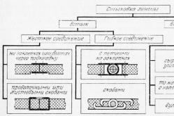
Construct a synchronous single-stage RS-trigger circuit on the NAND elements. Create a switching table. Using single-stage synchronic RS-flip-flops, draw a scheme of a two-stage RS-flip-flop. Explain the difference in work.
Each of the classification systems characterizes triggers in different indicators and therefore complements one another. For example, RS-type triggers can be synchronous and asynchronous performance.
Asynchronous the trigger changes its state directly at the moment of the appearance of the corresponding information signal (s), with some delay equal to the sum of the delays on the elements making up this trigger.
Synchronous The flip-flops respond to information signals only if there is an appropriate signal on the so-called clock input C (from the English clock). This entry is also referred to as the "tact". Such information signals are called synchronous. Synchronous triggers are in turn subdivided into triggers with static and with dynamic control at the synchronization input C.
Triggers with static control perceive information signals when fed to the input C of a logical unit (direct input) or logical zero (inverted input).
Triggers with dynamic control receive information signals when the signal at the input C changes from 0 to 1 (direct dynamic C-input) or from 1 to 0 (inverse dynamic C-input). Also called the "trigger triggered by the front".
Single-stage Triggers ( latch, latches) consist of a single stage representing a memory element and a control scheme, are, as a rule, with static control. Single-stage triggers with dynamic control are used in the first stage of two-stage triggers with dynamic control. A single-stage trigger on the UGO is designated by one letter - T.
Two-stage Triggers ( flip-flop, spanking) are divided into triggers with static control and triggers with dynamic control. At one signal level at input C, the information, in accordance with the logic of the trigger, is recorded in the first stage (the second stage is locked for recording).
At a different level of this signal, the state of the first stage is copied to the second stage (the first stage is locked for recording), the output signal appears at this time with a delay equal to the stage delay delay. Usually two-stage triggers are used in circuits where the logic functions of the trigger inputs depend on its outputs, in order to avoid temporary races. Two-stage trigger on the UGO is denoted by two letters - TT.
Triggers with complex logic there are also one- and two-stage. In addition to synchronous signals, there are asynchronous signals in these flip-flops. Such a trigger is shown in Fig. 1, the upper (S) and lower (R) input signals are asynchronous.

Fig. 2.39. Synchronous RS Triggers : synchronous RS-trigger on NAND elements and symbol;
The synchronous two-stage RS-trigger (master-slave, which translates "master assistant") consists of two synchronous RS-flip-flops and an inverter, Fig. 2.41, a. The inputs from both flip-flops are interconnected via an inverter DD1.1. If C = 1, then the first trigger functions according to the signals at its inputs S and R. The second trigger can not function, since it has C = 0. If C = 0, then the first trigger does not work, and for the second trigger C = 1, and it changes its state according to the signals at the outputs of the first trigger.

Fig. 2.41. Synchronous two-stage RS-flip-flop: a - trigger circuit on the AND gate; b - conventional designation and time diagrams of the clock pulse.
Principles of channel separation in methods of multiple-access access with frequency and time separation (FDMA and TDMA), their features and applications. Concepts on the construction of frames for BS and AS with TDMA.
Multiple access is typical for satellite channels, radio channels, mobile communication channels.
1. Technology FDMA (Frequency Division Multiple Access) performs manipulation of only one parameter of the information signal - frequency. Each channel has its own rather narrow band (20-25 KHz) in the frequency spectrum. Between these bands there are still additional frequency intervals - protective, reducing the interference of one channel to another. The difference between receiving and transmitting is also performed in frequency - FDD (Frequency Division Duplex). FDMA / FDD technology underlies analog cellular standards, for example NMT-450 and C-450.sub.b
The disadvantages of this method of channel separation are:
- narrowband information channel, and hence its sensitivity to selective fading (low noise immunity);
- irrational use of spectrum (band) frequency sections - difficulties in using the same spectral sections in the same territory.
The merits include the following:
- relative ease of implementation;
- high quality in the low-frequency part of the talk channel by such parameter as timbral color of speech (affects the recognizability of the speaker). In the absence of significant interference it is close to the quality in the channels of wired telephony.
2. TDMA (Time Division Multiple Access) technology already manipulates two parameters of the information signal - frequency and time. In this case, each channel is assigned a broader (with respect to FDMA) frequency band (up to 200 kHz), which in turn is divided into logical channels (time-separated). The difference between receive and transmit can be performed both in frequency - FDD (Frequency Division Duplex) and time TDD (Time Division Duplex). TDMA / FDD technology is used in digital cellular communication standards, for example GSM-900/1800 and D-AMPS. And TDMA / TDD technology underlies the DECT standard - digital wireless telephony.
The merits of this method include the following:
- higher noise immunity (compared to FDMA), achieved due to digitization of the information signal;
- the possibility of re-use of the same frequency bands in one territory - a higher reuse factor.
Disadvantages are:
- the remaining narrowband (relative), and as a result - susceptibility to selective fading, which manifests itself in the form of "croaking" and "gurgling" (loss of useful signal) in the low-frequency part of the conversation path;
- ineffective use of the frequency spectrum - the preservation of the frequency planning procedure.
Frequency Division Access (FDMA)FDMA is the simplest and most common method used in both analog and digital SSS. With FDMA, each AP transmits its signals in the allocated bandwidth of the repeater. The main disadvantage of FDMA is the reduction in bandwidth compared to single-signal mode, caused by the need to reduce by 4-6 dB the output power of the repeater amplifier due to the appearance of intermodulation jams. In addition, it is necessary to ensure a high stability of the frequency and power of the signal emitted by each AP.
In systems with FDMA, transmission can be performed by either multi-channel signals or single-channel signals using the "one channel on carrier" (OCN) transmission principle. The CCS method is used mainly in a network of stations with a small number of channels. The main advantage of the method is the possibility of implementing the principle of providing channels on demand. The FDMA method is widely used in the Intersputnik CAS, intelsat, national CAS of many countries. This method is difficult to use to connect a large number of computer subscriber stations and computer networks.
Time Division Access (TDMA)The TDMA method was applied in connection with the implementation of digital transmission methods. In this method of each 3C, a definite periodically repeated time interval is allocated for the emission of signals. The radiation intervals of all stations are mutually synchronized, so that they do not overlap. At each moment of time, only one station passes through the repeater and there is no non-linear interaction of the signals of different 3Cs in the repeater amplifier.
The TDMA method is developed for the transmission of data from a large number of subscriber stations connected to the digital telephone network and by means of the channel multiplexing equipment, transmission through the main APs is carried out. It is used to connect a large number of autonomous computer subscriber stations and computer networks with direct communication with the satellite station, significant costs are required with limited capabilities according to the number of APs.
Frame The TDMA consists of four subframes (windows). Multi-shot contains 18 frames, hyperframe -50 multi-frames. The frame duration is 53.37 ms, the multiframe is 1.02 s. In each frequency channel, four physical channels are organized with frequency spacing between 25 kHz channels or two channels with a frequency separation of 12.5 kHz.
A packet containing 510 bits is transmitted in the window. There are six typical packages: NUB -standard package for the upward direction (Fig.9.2, a); NDB - a standard package for a downward direction (Fig.9.2, b); SB - synchronization package for the AS (Figure 9.2.c); single standard package for downward direction; a single synchronization package for the speaker and a management pack.

Standard packets are designed to transmit traffic and control channel information. Single packages - for the same purposes. Only they are used in time division modes, for example, with time division of channels between zones in a developed system. The control package (Figure 9-2. G and d) consists of two independent semi-packages: up (LB) and down (CB). LB - power control signal half packet. It only takes one (left) half-pack. CB is a half-packet of the power control channel. It takes one half-packet, but can be transmitted in any of them (left and right).
The structure of the packet (Figure 9.2) is formed by the following fields and bits:
P - power control bit;
01 - standard training sequence;
02 - extended training sequence;
F - bits of phase adjustment;
F - frequency correction bits;
S is a synchronization sequence.
The fields for the transmission of the traffic channel information and the control channel are indicated by the INF and I2, where the INF means that this field can occupy the bits of any of these channels, and the I2 only the control channel. One feature in Fig. 9.2 crossed out the fields for the transition bits, two traits - protective time intervals. In Fig. 9.2 indicates the number of bits of each field.
Training sequences serve to adjust the equalizer, maintain frame synchronization of packets, and transmit information about the structure of the packet. There are three standard training sequences of 22 bits and one extended training sequence - 30 bits. Two of them indicate that one or two logical channels are transmitted in the standard packet.
The autocorrelation functions of the signals of the training sequence have one peak width one clock interval and a small level of lateral components. This allows you to reliably determine the beginning of the sequence at the reception to maintain frame synchronization. By the form of the interrelationship function, you can confidently distinguish the sequences.
The protective time interval is entered in single packets to reduce inter-channel interference. During this interval, the carrier is not radiated. The phase adjustment bits serve to restore the initial phase of the carrier. A field of 80 bits is provided for frequency correction. In this field three radio pulses with known frequencies are formed.
Rectifier diodes Semiconductor devices with one p-n junction are called. The main property that underlies the operation of rectifier diodes - one - sided conductivity. An example of such a diode is shown in Figure 1.
Figure 1. Volt-ampere characteristic of a rectifier diode.
Volt-ampere characteristic of a rectifier diode
The figure in the first quadrant is a straight line, in the third - the reverse branch of the diode characteristic. The direct branch of the characteristic is removed under the action of a forward voltage, the inverse of the reverse voltage on the diode. Direct voltage on a diode is called such that a higher electric potential is generated at the cathode with respect to the anode , and if you speak in the language of signs - at the cathode minus (-), at the anode plus (+) , as shown in Figure 2.
Figure 2. Diagram for studying the current-voltage characteristics of a diode in direct connection.
Figure 1 shows the following conventions:
Ip - operating current of the diode;
Ud - voltage drop across the diode;
Uo - reverse diode voltage;
Upr - Breakdown voltage;
Iy - leakage current, or reverse diode current.
Concepts and designations of characteristics
Operating current of the diode (Ip) , this is a direct, long time passing through a diode, in which the device is not subjected to irreversible temperature destruction, and its characteristics do not undergo significant qualitative changes. In directories can be indicated as a direct maximum current.
on the diode (Ud) - voltage across the terminals of the diode, which occurs when a direct working current passes through it. In directories can be designated as direct voltage on the diode.
Direct current flows when the diode is directly connected .
The reverse voltage of the diode (U0) - permissible reverse voltage on the diode, applied to it for a long time, at which irreversible destruction of its p-n junction does not occur. In the reference literature can be called the maximum reverse voltage.
Breakdown voltage (Upr) - reverse voltage on the diode at which an irreversible electrical breakdown p-n transition, and, as a consequence, the failure of the device.
The reverse current of the diode, or leakage current (Iu) - reverse current, long time does not cause irreversible destruction (breakdown) of the p-n junction of the diode.
When choosing rectifier diodes, they are usually guided by the above mentioned characteristics.
Diode operation
Subtleties the work of p-n transition, the topic of a separate article. We simplify the problem, and consider the operation of the diode from the position of one-sided conductivity. So, the diode works as a conductor in a straight line, and as a dielectric (insulator) when it is turned on again. Consider the two schemes in Figure 3.
Figure 3. Inverse (a) and direct (b) diode inclusion.
The figure shows two variants of one scheme. In Fig. 3 (a), the position of the switches S1 and S2 provides electrical contact of the diode anode with the minus of the power source, and the cathode through the lamp HL1 with a plus. As we have already decided, this reverse diode inclusion. In this mode the diode will behave like an electrically insulating element, the electrical circuit will be practically open, the lamp will not burn.
When the position of the contacts S1 and S2 is changed, Fig. 3 (b), the anode of the diode VD1 is electrically contacted with the positive of the power source, and the cathode through the light bulb is connected with a minus. Wherein the condition of direct switching on of the diode is fulfilled, it "opens" and through it, as through a conductor, the load current (of the lamp) flows.
If you have just started to study electronics, you can be a little confused by the complexity of the switches in Figure 3. Draw an analogy from the description given above, based on the simplified diagrams in Figure 4. This exercise will allow you to understand and navigate a little about the principle of building and reading electrical circuits.
Figure 4. Diagram of reverse and direct inclusion of the diode (simplified).
In Figure 4, the polarity reversal at the diode leads is provided by changing the diode position (by turning).
Unidirectional conductivity of a diode
It can be seen that the synchronous change in the positions of the switches S1 and S2 (Figure 3) simulates the feeding of a diode lamp to the series circuit Figure 5.
Figure 5. Voltage diagrams before and after the rectifier diode.
We assume conditionally that the electric potential of switch S2 is always 0. Then the voltage difference will be applied to the anode of the diode -US1-S2 and + US1-S2 depending on the position of the switches S1 and S2. The diagram of such alternating voltage of a rectangular shape is shown in Figure 5 (upper diagram). With a negative voltage difference at the diode anode, it is locked (it works as an isolating element), while through the lamp HL1, the current does not flow and it does not burn, but the voltage on the lamp is practically zero . With a positive voltage difference, the diode opens (acts as electrical conductor) and a current flows through a series of diode-lamp circuits. The voltage on the lamp increases to UHL1. This voltage is slightly less than the power supply voltage, since part of the voltage drops on the diode . For this reason, the voltage difference in electronics and electrical engineering is sometimes called "voltage drop". Those. in this case, if the lamp is viewed as a load, then it will be load voltage, and on the diode - voltage drop.
In this way, the periods of the negative voltage difference are ignored by the diode, cut off, and the current flows only through the load during periods of positive voltage difference. This transformation of alternating voltage into unipolar (pulsating or constant) is called rectification.
And as there is a current in it. Today we will continue the topic started and talk about principle of operation of semiconductor diodes.
Diode Is a semiconductor device with one p-n a transition having two terminals (an anode and a cathode), and intended for rectification, detection, stabilization, modulation, limitation and conversion of electrical signals.
According to their functional purpose, diodes are divided into rectifying, universal, pulse, microwave diodes, zener diodes, varicaps, switching, tunnel diodes, etc.
Theoretically, we know that a diode in one direction passes current, and the other does not. But how and how he does it, many people do not understand and understand.
Schematically, a diode can be represented as a crystal consisting of two semiconductors (regions). One region of the crystal has a conductivity ptype, and the other conductivity n-type.

On the image holes, prevailing in the region p-type, are conventionally depicted in red circles, and electrons, prevailing in the region n-type - blue. These two regions are the electrodes of the diode anode and cathode:
Anode - positive electrode holes.
Cathode - negative electrode diode in which the main charge carriers are electrons.
On the outer surfaces of the areas are contact metal layers, to which are soldered wire conclusions the electrodes of the diode. Such a device can only be in one of two states:
1. Open - when it conducts a current well;
2. Closed - when it conducts a current badly.
Direct connection of the diode. Direct current.
If a constant voltage source is connected to the diode electrodes: to the anode terminal " a plus"And on the cathode output" minus", The diode will be in open a current will flow through it, the value of which will depend on the applied voltage and the properties of the diode.
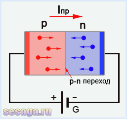
With such polarity of connection, electrons from the region n-type will rush to meet the holes in the region ptype, and holes from the region ptype will move towards electrons in the region n-type. At the interface of the regions, called electron-hole or p-n transition, they will meet, where their mutual absorption takes place or recombination.
For example. The main charge carriers in the region ntype of electrons, overcoming p-n the transition falls into the hole region p-type in which they become non-core. Became non-basic, electrons will be absorbed major carriers in the hole region - holes. In the same way, holes entering the electronic region n-type become non-core carriers in this region, and will also be absorbed major carriers - electrons.
The diode contact coupled to negative pole of the DC voltage source will be give away field of n-type practically unlimited number of electrons, replenishing the decrease of electrons in this region. A contact connected to positive pole of the voltage source, is capable of to accept from the region ptype, the same number of electrons, due to which the hole concentration in the region p-type. Thus, the conductivity p-n transition will big and current resistance will be few, and therefore a current will flow through the diode, called direct current diode Ipr.
Reverse inclusion of the diode. Reverse current.
Let us change the polarity of the DC voltage source - the diode will be in closed condition.

In this case, the electrons in the region ntype will move to positive pole of the power source, moving away from p-n transition, and a hole, in the region ptype, will also be separated from p-n go to negative pole of the power source. As a result, the boundaries of the regions seem to expand, causing the formation of a zone depleted of holes and electrons, which will exert a current great resistance.
But, since in each region of the diode there are non-core charge carriers, then a small exchange of electrons and holes between regions will still occur. Therefore, a current that is many times smaller than a straight line will flow through the diode, and such a current is called reverse current diode ( Iobr). As a rule, in practice, the reverse current p-n transition are neglected, and this leads to the conclusion that p-n transition has only unidirectional conductivity.
Forward and reverse diode voltage.
The voltage at which the diode opens and through it a direct current is called direct (Upr), and the reverse polarity voltage at which the diode closes and through it the reverse current is called reverse (UOBR).
With direct voltage ( Upr) the resistance of the diode does not exceed a few tens of Ohms, but with a reverse voltage ( UOBR) the resistance increases to several tens, hundreds and even thousands of kilograms. This is not difficult to verify if you measure the reverse resistance of the diode with an ohmmeter.
Resistance p-n transition of the diode is not constant and depends on the forward voltage ( Upr), which is fed to the diode. Than more this tension, the less resistance has p-n transition, the more forward current Ipr flows through a diode. In the closed state on the diode falls practically all the voltage, therefore, the reverse current passing through it small, and resistance p-n transition is great.
For example. If the diode is connected to an alternating current circuit, it will open at positive half-periods on the anode, freely flowing forward current (Ipr), and close at negative half-periods at the anode, almost without passing current of the opposite direction - back current (Iob). These properties of diodes are used for aC to DC conversion, and such diodes are called rectifying.
Volt-ampere characteristic of a semiconductor diode.
The dependence of the current passing through p-n the transition from the magnitude and polarity of the voltage applied to it is represented in the form of a curve called current-voltage characteristic of a diode.
The graph below shows such a curve. By vertical axes in the upper part indicate the values of the forward current ( Ipr), and in the lower part - reverse current ( Iobr).
By horizontal axis on the right side denotes the values of the forward voltage Upr, and in the left part - the reverse voltage ( UOBR).
The current-voltage characteristic consists of two branches: straight branch, in the right upper part, corresponds to the direct (throughput) current through the diode, and backward branch, in the left lower part, corresponding to the reverse (closed) current through the diode.

Straight branch goes up steeply, snuggling up to vertical axis, and characterizes the rapid growth of the forward current through the diode with increasing forward voltage.
The reverse branch goes almost in parallel horizontal axis and characterizes the slow growth of the reverse current. The steeper the straight line to the vertical axis and the closer to the horizontal the reverse branch, the better is the rectifying properties of the diode. The presence of a small reverse current is a disadvantage of diodes. From the curve of the current-voltage characteristic it can be seen that the direct current of the diode Ipr) is hundreds of times the reverse current ( Iobr).
When the forward voltage is increased through p-n the transition of the current first increases slowly, and then a section of rapid current rise begins. This is explained by germanium the diode opens and starts to conduct a current at a forward voltage of 0.1 - 0.2V, and silicic at 0.5 - 0.6V.
For example. With direct voltage Upr = 0.5V forward current Ipr is equal to 50mA (point " a"On the graph), and already at a voltage Upr = 1V current increases to 150mA (point " b"On the graph).
But such an increase in current leads to a heating of the semiconductor molecule. And if the amount of heat released is more than the one taken away from the crystal in a natural way, or with the help of special cooling devices ( radiators), then in the conductor molecule irreversible changes can occur up to the destruction of the crystal lattice. Therefore, the forward current p-n transition limit at a level that excludes overheating of the semiconductor structure. To do this, use a limiting resistor, connected in series with the diode.
For semiconductor diodes, the value of the forward voltage Upr at all values of working currents does not exceed:
for germanium - 1B;
for silicon - 1,5V.
With increasing reverse voltage ( UOBR) attached to p-n transition, the current increases insignificantly, as indicated by the inverse branch of the current-voltage characteristic.
For example. We take a diode with the following parameters: Max max = 100V, Iob max = 0.5 mA, where:
Max max - maximum constant reverse voltage, V;
Iob max - maximum reverse current, μA.
With a gradual increase in the reverse voltage to a value of 100V, it is seen how the back current is growing insignificantly (point " at"On the graph). But with a further increase in the voltage, above the maximum, which is calculated p-n transition of the diode, there is a sharp increase in the reverse current (dotted line), heating of the semiconductor crystal and, as a consequence, breakdown p-n junction.
Breakdowns of the p-n junction.
Breakdown p-n transition is the phenomenon of a sharp increase in the reverse current when the reverse voltage reaches a certain critical value. Distinguished electric and thermal breakdowns p-n transition. In turn, the electrical breakdown is divided into tunnel and avalanche breakdowns.

Electrical breakdown.
Electrical breakdown occurs as a result of the impact of a strong electric field at p-n transition. Such a breakdown is reversible, that is, it does not lead to damage to the transition, and when the reverse voltage decreases, the properties of the diode remain. For example. In this mode work zener diodes - diodes designed to stabilize the voltage.
Tunnel breakdown.
Tunnel breakdown occurs as a result of the phenomenon tunnel effect, which manifests itself in the fact that with a strong electric field strength acting in p-n transition small thickness, some electrons penetrate (leak) through the transition from the region p-type in the region n-type without change their energy. Thin p-n Transitions are possible only at high concentrations impurities in the semiconductor molecule.
Depending on the power and purpose of the diode, the thickness of the electron-hole junction can be in the range from 100 nm (nanometers) to 1 micron (micrometer).
Sharp growth is characteristic of tunnel breakdown reverse current with little reverse voltage - usually a few volts. Based on this effect work tunnel diodes.
Due to their properties, tunnel diodes are used in amplifiers, sinusoidal relaxation oscillators and switching devices at frequencies up to hundreds and thousands of megahertz.
Avalanche breakdown.
The avalanche breakdown consists in the fact that under the action of a strong electric field non-core charge carriers under action heat at p-n transition are accelerated by as many as are capable of knock out from the atom one of its valence electrons and throw over it into the conduction band, forming a pair electron-hole. The charge carriers formed also begin to accelerate and collide with other atoms, forming the following electron-hole pairs. The process becomes avalanche-like, which leads to a sharp increase reverse current at practically unchanged tension.
Diodes, which use the effect of avalanche breakdown are used in powerful rectifier units, used in the metallurgical and chemical industry, railway transport and in other electrical products, in which the reverse voltage may be higher than permissible.
Thermal breakdown.
Thermal breakdown occurs as a result of overheating p-n transition at the moment of current flow through it a large values and inadequate heat sink that does not ensure the stability of the thermal transition regime.
When increase appended to p-n transition of reverse voltage ( UOBR) power dissipation at the transition is growing. This leads to increase the transition temperature and adjacent regions of the semiconductor, intensify vibrations of crystal atoms, and wanes the bond of valence electrons to them. There is a probability transition electrons into the conduction and formation zone additional electron - hole pairs. Under bad conditions heat transfer from p-n transition occurs avalanche increase in temperature, which leads to destruction transition.
On this let's finish, and in part we will consider the device and operation of rectifier diodes, a diode bridge.
Good luck!
Diodes are often referred to as "direct" and "reverse". What is the reason for this? What is the difference between a "direct" diode and an "inverse" diode?
What is a "direct" diode?
A diode is a semiconductor with 2 terminals, namely an anode and a cathode. It is used for processing different ways electrical signals. For example, in order to straighten, stabilize, transform.
The peculiarity of the diode is that it transmits current only in one direction. In the opposite direction - no. This is possible due to the fact that in the structure of the diode there are 2 types of semiconductor regions that differ in conductivity. The first conditionally corresponds to an anode having a positive charge, the carriers of which are so-called holes. The second is a cathode that has a negative charge, its carriers are electrons.
The diode can function in two modes:
- open;
- closed.
In the first case, a current flows well through the diode. In the second mode - with difficulty.
Open the diode by direct switching. To do this, connect the positive wire from the current source to the anode, and negative to the cathode.
Direct also can be referred to as diode voltage. Unofficially, the semiconductor device itself. Thus, "direct" is not he, but a connection to it or tension. But for simplicity of understanding in electrical "direct" is often called the diode itself.
What is a "reverse" diode?
The semiconductor is closed by means of, in turn, a reverse voltage supply. To do this, change the polarity of the wires from the power source. As in the case of a direct diode, an inverse voltage is formed. "Reverse" - by analogy with the previous scenario - is called the diode itself.
Comparison
The main difference between the "direct" diode and the "reverse" diode is the way the current is fed to the semiconductor. If it is fed for the purpose of opening a diode, the semiconductor becomes "direct". If the polarity of the wires from the current source changes - then the semiconductor closes and becomes "inverse".
Considering the difference between a "direct" diode and an "inverse" diode, we will reflect the main conclusions in the table.
In total, with one p-n junction, which has two external terminals, the anode and the cathode. It is used for rectification, detection, modulation, limitation and various types of conversion of electrical signals. For functional purposes, diodes are classified into rectifier, universal, microwave, zener diode, pulse, varicaps, varistors, switching, tunneling etc.

Structurally, a diode can be represented by a semiconductor crystal consisting of two regions. One with conductivity ptype, and the other conductivity n-type.

Diode operation explanatory structural diagram
The anode is a plus electrode, in which the main charge carriers are holes.
The cathode is a negative electrode, in which the main charge carriers are electrons.
On the outer surfaces of the two regions there are contact metal layers to which the outer terminals are soldered. Such a semiconductor device can only be in one of two states: open and closed
If the terminals of a semiconductor device are connected constant pressure: the anode is applied plus and the output of the cathode is correspondingly minus, then the diode opens and a current starts flowing through it, the magnitude of which depends on the applied voltage and internal properties of the diode.

With direct inclusion, electrons from the n region will move toward the holes in the p-region, and the holes from p to the region n. At the boundary of the electron-hole transition, they will meet, and their mutual absorption or recombination will occur.
The output of the diode, connected to the minus, will send a huge number of electrons to the region n, replenishing their decrease. A pin connected to a plus helps to restore the hole concentration in the p region. That is, the conductivity of the electron-hole junction increases, and the resistance to the current decreases sharply, and therefore a current flows through the diode, called the forward current of the diode Ipr.
Change the polarity of our connection and look at the changes in the operation of the connected semiconductor device.

In this case, electrons and holes will be pushed away from the pn junction, and at the boundary of the electron-hole junction, the potential barrier sharply increases, or in other words, the band depleted of charge carriers by electrons and holes that will impede the passage of current.
But, since in each of the regions there is a small number of minority carriers, a small exchange of charge carriers between the regions still occurs, but it is very small. This current is called the reverse current Iobr.
Diode operation direct and reverse voltage |
The voltage, the opening of the diode, when a direct current flows through it, is called the direct Up, and the voltage of the reverse polarity at which it is locked and through it flows is called the inverse U, At U pr, the internal resistance is not higher than a few tens of Ohms, but at U the resistance sharply increases to hundreds and even thousands of kilograms. This is easy to see if you measure the reverse resistance using a multimeter.
The resistance of the electron-hole transition is not constant and depends on Upr. The higher it is, the less resistance p-n transition, the higher Iper going through the semiconductor. In the closed state, almost all the voltage falls on it, therefore, Ip is negligibly small, and the resistance of the p-n junction is enormous.
If we connect the diode to the alternating current circuit, it will be opened with positive half-wave sinusoidal voltage, passing the forward current, and locked with a negative half-wave, almost without passing the IOp. This main property of diodes is used to convert AC voltage to DC, and such devices are called rectifiers.
The dependence of the current passing through the electron-hole junction on the magnitude and polarity of the voltage is represented in the form of a curve called the current-voltage characteristic
It consists of two branches: a straight branch corresponds to a direct current through a diode, and an inverse branch corresponding to the reverse current.

The direct branch of the graph rises steeply upward and characterizes the rapid growth of the forward current with increasing value of the forward voltage. The back branch, on the contrary follows almost parallel to the horizontal axis, and characterizes the slow growth of the I model. The closer the straight line to the vertical axis and the closer to the horizontal axis the reverse branch, the better the rectifying properties of the semiconductor. The presence of Iob is a disadvantage. It can be seen from the curve of the I-V characteristic that I is much larger than the I sample.
As we see from the graph with increasing forward voltage through the electron-hole transition, the current initially increases slowly, and then much faster.
But such a sharp increase in current heats the molecules of the semiconductor. And if the amount of heat is higher than the amount removed from the crystal, irreversible changes and destruction of the crystal lattice can occur.
Therefore, it is necessary to use the limiting resistance included in series.
With a strong increase in the reverse voltage, a breakdown of the electron-hole device can occur. Even there are special semiconductor devices called zener diodes in which this property is applied.
The work of the diode is a p-n junction breakdown |
Breakdown of the pn junction is a phenomenon of a sharp increase in the reverse current when the reverse voltage reaches a certain critical level. Thermal breakdowns in turn are divided into electrical and thermal, and electrical breakdown is tunnel and avalanche.

Electrical breakdown occurs as a result of the action of a strong electric field in the transition. Such a breakdown is considered reversible, since it does not lead to damage to the crystal, and when the reverse voltage level decreases, the characteristics of the diode remain.
Tunnel breakdown It results from the tunneling effect, which consists in the fact that at a high electric field strength in narrow p-n transition, individual electrons percolate through the transition. Such pn transitions are possible only under conditions of a high concentration of impurities in the semiconductor molecule.
In the case of tunnel breakdown, there is a sharp increase in Iob with a small reverse voltage. Based on this property, tunnel diodes were developed. They are used in amplifiers, sinusoidal oscillators and in various switching devices at high frequencies.
Avalanche breakdown also occurs under the action of a strong electric field, when the minority charge carriers under the influence of heat in the transition are accelerated by so much that one of the valence electrons is knocked out of the atom and thrown into the conduction band, creating an electron-hole pair. The resulting free carriers begin to accelerate and collide with other atoms, knocking out other electrons. The process is avalanche-like, which leads to a sharp increase in I arr at practically unchanged voltage level.
The effect of avalanche breakdown is used in powerful rectifier units used in the metallurgical and chemical industries, as well as in railway transport.
Thermal breakdown is due to overheating of the p-n junction during the flow of a large current level, and with poor heat removal. This leads to a sharp increase in the transition temperature and neighboring regions, the vibrations of the atoms of the crystal structure increase, and the bond of the valence electrons disappears. Electrons begin to flow into the conduction band, an avalanche-like increase in temperature occurs, which leads to the destruction of the crystal and the failure of the radio component.
Description of the operation of a rectifier on semiconductor diodes
Principle of work of a zener diode
Stabilitron - a kind of semiconductor diode, operating at reverse bias voltage in the breakdown mode. Until the moment of the breakdown, very small leakage currents flow through the zener diode, and its resistance is quite high. At the moment of breakdown, the current through it sharply increases, and its differential resistance decreases to small values. Due to this in the breakdown mode, the voltage on the zener diode is maintained with good accuracy in a large range of reverse currents.