Antipyretics for children are prescribed by a pediatrician. But there are situations of emergency care for fever, when the child needs to give the medicine immediately. Then the parents take responsibility and apply antipyretic drugs. What is allowed to give to infants? How can you bring down the temperature in older children? Which medications are the safest?
The general trend of electronics development over the past 50 years is an increase in complexity and cheaper. If in 1950 the radio set was so expensive that the engineer's monthly salary could not be enough to buy it, today a hundred radio receivers can be bought for an average salary. Reduction is possible only due to a change in design in such a way that the amount of manual labor is minimized. Let's see how the appearance of the electronic blocks changed.
Historically, the very first technology is the so-called volumetric mounting or hinged mounting. Radioelements are soldered to the rows of special petals, and are connected to each other by wires connected in bundles.
Assembly completely manually, to automate the process of such assembly is difficult. Another option is possible, when the petals are arranged differently:
Packing density is minimal, resistance to shocks and vibrations is also low.
For example, a measuring device made using the technology of surface mounting:


The labor capacity of assembling such devices can be imagined.
Then the engineers had an idea. If the radio components are connected in a special way in the device, then it is possible in some mass way to make this connection drawing pattern in advance from the conductor, and simply fix the parts in the right places, they will be connected automatically in the correct order. So printed circuit boards appeared.
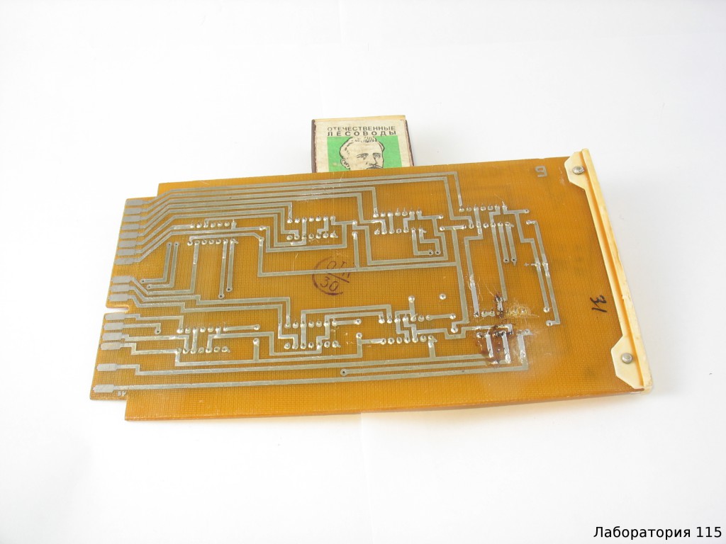
A printed circuit board is a plate made of a getinax or fiberglass, on which a copper foil pattern with holes for the terminals of radio elements is applied. Radio components are simply inserted into the holes and soldered to the foil pattern. The beauty of this method is that, firstly, the plates with a pattern can be made massively by etching, and secondly, with certain improvements, you can solder all the elements to the board at once, dipping the entire board into molten solder.
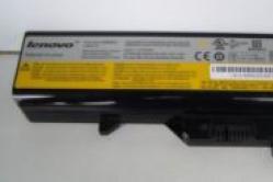
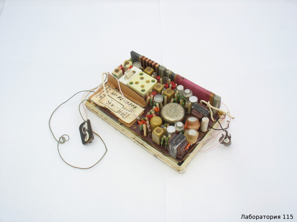
Here is an example of a radio receiver with a printed circuit board. You can see that the details are packed pretty tightly.
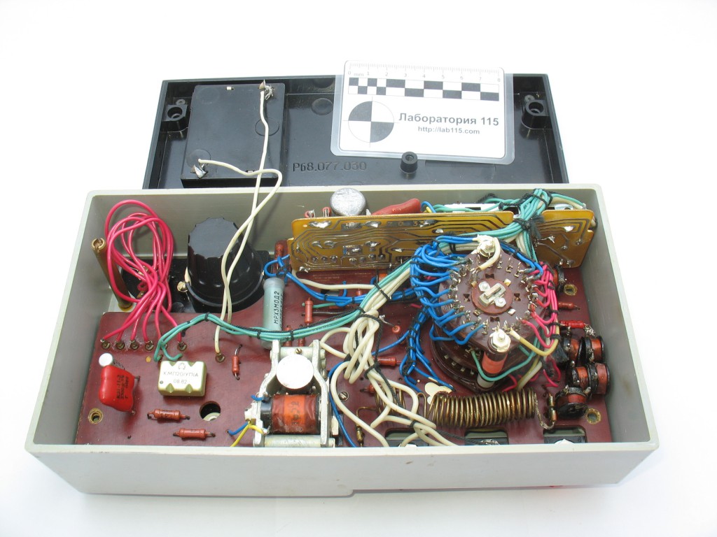
The measuring device has become more compact inside the switch to printed mounting:
And in the next generation is even more compact:

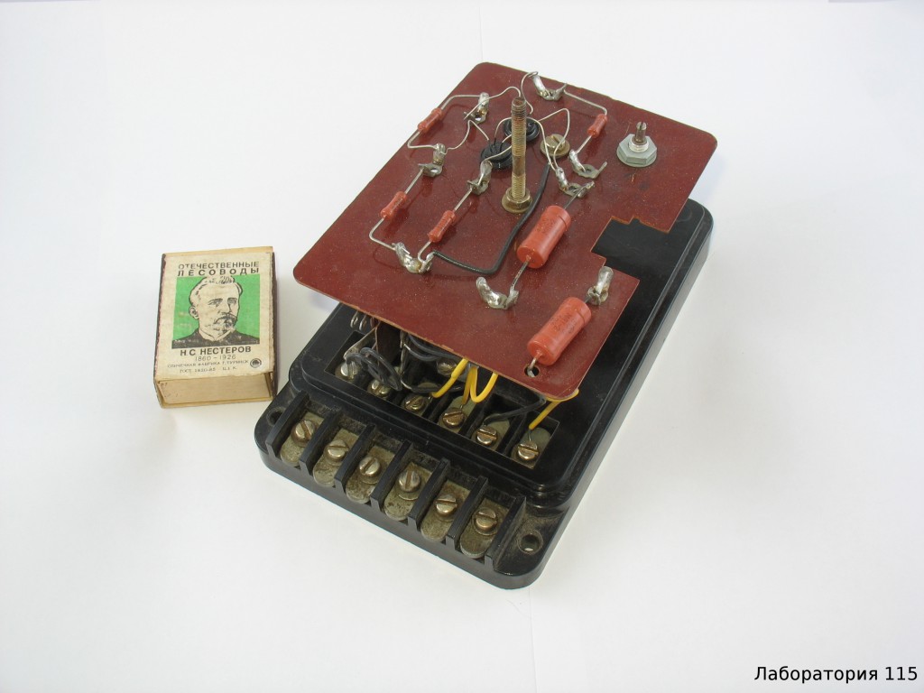
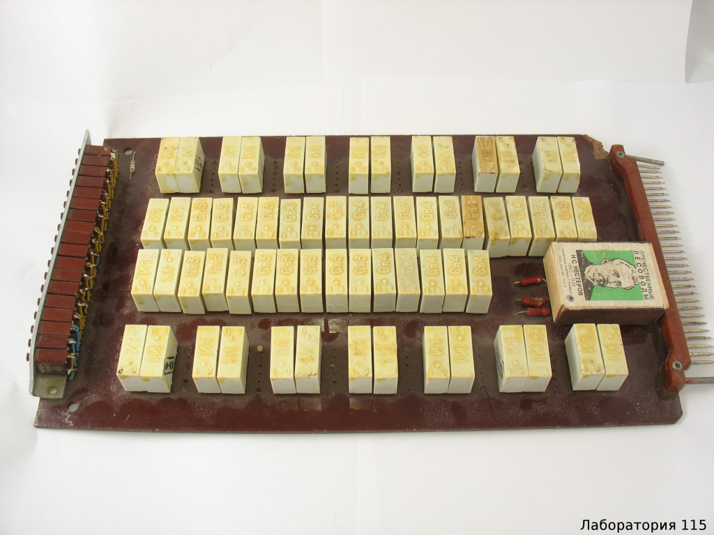
In parallel with the development of PCB technology, microminiaturization has evolved. The elements themselves became more compact due to the appearance of semiconductor elements and the transition to low voltage power supply. Then the elements themselves began to assemble in factories in microassemblies, micromodules, and eventually chips appeared. With the increase in the packing density of the elements in the body of the assemblies, the drawing of the connection of the parts on the board became denser and eventually it became impossible to fit it on the plane without intersections. Here is an example of a block built on microassemblies, in which, in addition to the printed drawing, jumpers are used:

But jumpers require soldering manually. The next stage was the placement of a conducting pattern of copper foil on both sides. Here is an example with microcircuits:

Attentive readers could notice that when creating a printed circuit board with a two-sided drawing, there appeared tracks that through the hole "dive" to the other side. This so-called transition holes. Their creation is not so simple, and if a simple one-way circuit board can be made at home, it is difficult to make a double-sided printed circuit board with vias because the walls of the hole must be covered with a layer of copper that is grown galvanically. The process of manufacturing the boards will be discussed in another article.
Later the elements became even smaller, their packaging became even denser. Appeared surface mount technology, when the part was soldered onto the tracks with its entire body, and not through the wire leads passed through the holes in the board and soldered to the conductors from the back side. In this case, the elements are placed in the right place by the robot and the printed circuit board can be made completely automatically.

To reduce the cost and reduce the size of the crystals of chips began to be attached directly to the board, pouring compound. You could see such black drops on the PCB. Here is a chip chip not filled with compound:

It became impossible to perform all necessary connections using only two layers of conductors, so they began to do multi-layer printed circuit boards. They are more expensive, more difficult to manufacture, they try to do without them, but not always it is possible. Photo of the computer motherboard cut:

It is seen that in addition to the outer layers with conductors there are two internal layers. And the holes have a metallization.
As a result, what we can observe is that electronic components become cheaper and more compact due to the transition from manual labor to automatic group assembly technologies. Automation is the only way to improve the well-being of every person due to a significant reduction in the cost of production of things. The placement of assembly plants in countries with cheap labor will only give a temporary, insignificant effect.
- relative permittivity;
S is the area of the plates (mm2);
d is the distance between the plates;
n is the number of plates.
There are materials whose permittivity depends on the applied voltage. A capacitor with dielectrics based on such materials is a varicon. There are capacitors using p-n properties transition, changing its width depending on the applied voltage. P-n junction in the capacitor is used as a dielectric - varicap.
Basic parameters of the capacitor (characteristic)
1. The value of the nominal capacity - determines the capacity of the capacitor, which depends on the geometric dimensions of the plates, the type of dielectric constant and the distance between the plates (the larger it is, the smaller the capacity).
In principle, the capacitance of the capacitor from 1 to 9999 pF indicates integers in the corresponding value of the capacity, and from 10,000 pF and higher - in μF or in fractions. If the capacity is equal to an integer number of μF, then the last digit is set to zero.
1F - capacity a solitary explorer potentially increases by 1c with an increase in charge by 1C.
2. Condenser Accuracy Class - tolerance;
3. Operating voltage is the voltage at which the capacitor can operate for a long time without breakdown of the dielectric. The operating voltage depends on the properties and thickness of the dielectric;
4. temperature coefficient of capacity - characterizes the relative change in the capacity of the condenser at a temperature equal to 1 ° C.
TKE - negative and positive.
5. Insulation resistance - characterizes the quality of the dielectric and the magnitude of the leakage current through it, largely depends on the temperature and humidity of the environment.
Installation and use of a capacitor
1) clamps;
2) with screws;
3) by gluing and soldering;
4) with nuts.
Terminology
A thread resistor is a resistor whose linear dimension along the axis is much larger than its diameter.
Posistor - PP-thermistor with positive TCR.
Polar capacitor - designed for use in circuits of constant and pulsating current with a certain polarity of voltage at its terminals. Dielectric is an oxide film formed on the surface of aluminum or tantalum film, the plates are a film or a viscous electrolyte.
Varikap - PP diode with a capacity that depends on the applied voltage and is intended for use as an element with an electrically controlled capacitance.
Varicond is a ferroelectric ceramic capacitor with a sharply nonlinear dependence on the applied voltage.
Types of wiring, printed wiring
lectremontage - assembly of products from parts, assemblies and their connections.
1) For bulk installation, the parts are located inside the frame using the entire space inside the frame;
2) With free installation large parts are placed on the flat part of the REA;
3) Block installation - installation, in which the radio device consists of certain units and units that have their own frames and are connected together by wires with their connectors.
Printed Mounting
The main brands of wires and insulating materials. Technical manufacture of printed circuit boards.
Modern REAiP apply the following types of installation:
1. Free (planar);
With free installation, large parts are placed on a flat chassis of radio equipment.
2. Volumetric;
With bulk mounting, the parts are located inside the frame using the entire space inside the frame.
3. Block;
Block installation - installation, in which the radio device consists of certain blocks and units that have their own frames and are connected together by wires with their connectors.
4. Printed.
Printed installation is its advantages:
1) the reduced mass and dimensions of the equipment;
2) the process of production of REA is accelerated and simplified;
3) its mechanical strength and stability increase.
Structurally, technological requirements for electrical installation
The electrical installation of the REA is carried out in accordance with the requirements set forth in the assembly drawings, technical documentation and in accordance with the requirements of the established standard (sample).
The installation should ensure normal operation of the equipment in conditions of shaking, vibration, vacuum, high humidity, exposure to positive and negative temperatures caused by the requirements of the relevant technical conditions for the installed equipment or device. The design and electrical installation of REA should provide access to individual elements for their inspection, verification and replacement.
The marking marks on the chassis of the instrument should not be covered as far as possible by mounting wires. For the installation of REAiP, wires are used, the marks of which, cross-section and coloring are indicated in the drawings or diagrams. Marking should be different from each other. The method of marking is indicated in the drawings. Soldering in the joint and overlap is not allowed. Connections longer than 30mm are made with an insulated wire, and less than 30mm with a bare wire enclosed in an insulating tube. All elements of the CEA are arranged so as to exclude the possibility of overheating of some elements from others.
Wires
Materials used in the installation work include various cable products - bare and insulated. Designed for transmission electric current. Both insulated and bare wires can be single-core and stranded. When installing high-frequency equipment units, use a copper bare wire covered with a layer of silver. Copper tinned wire is often used.
Insulating materials and their applications
1. Textolite, getinaks - used for the manufacture of boards, panels, gaskets, coil frames, low-frequency transformers, mounting racks ...
2. Organic glass - used for the manufacture of scales, transparent screens, decorative elements.
3. Polyvinyl chloride - used for the manufacture of insulating pads, insulation of wires.
4. Polystyrene - inductance coil frameworks, panels, mounting parts, insulation of high-frequency cables.
5. Teflon - inductance coil frameworks, panels, mounting parts, insulation of high-frequency cables.
6. Electro and radiopharmor - insulators, switches, aisles, insulating sleeves ...
Fabrication and laying of harnesses
The harness (one-piece and two-block) is a set of divided cable wires that are fastened to each other in some way and if necessary equipped with wiring elements.
1. In-block - for connecting separate units, blocks and parts inside the device.
2. Inter-unit - for an elementary connection between blocks.
It is recommended to make bundles on templates. The ends of the wires of the harness are marked according to the assembly drawing and the wiring diagram. The length of the harness leads must be sufficient to connect to the nodes and elements of the circuit without tension, in addition, there must be a margin of 10-12 mm for re-stripping and attaching each end of the wire.
Details Author: EngineerDeveloper®When using DIP-type enclosures and passive terminal housings, first of all, there are mounting holes for their mounting. This type of component is used in cases where there are no requirements for the dimensions of the printed circuit board of the developed device. Usually such installation is used to reduce the cost of development. But the price, as a rule, becomes cheaper, but the difference with planar editing remains not great. This is explained by the large number of holes in the holes.
In the case of using the mounted mounting, the overall dimensions of the board and the length of the conductors are substantially increased, which will not allow the device to operate at high frequencies. Therefore, hinged installation is not recommended for use in the development of high-frequency devices, as well as analog devices located near high-speed logic circuits.
Some developers in order to reduce the length of the conductors have the resistors upright. But at such inclusion of a component the way of passage of a current through the resistor increases, and the resistor represents a loop (a coil of inductance). In this case, the radiation power of this component increases. Also, a component with such an inclusion is induced by a large amount of noise and noise.
No planar (surface) mounting is required. However, there are difficulties in setting up and testing, installation. Those. there is a need to install additional control points. But with surface mounting, the mutual influence of components on the RF can be minimized. Similarly, the laboriousness of installation increases with the use of a small component size.
The installation of a radio means the connection, in accordance with the principal electrical circuit, of individual radio components to the finished product. There are special rules for mounting each type of radio components, which can be found either in the technical conditions for this type of parts, or in radio amateur reference literature. In this book, I will not deal with the rules for installing various radio components, but only very briefly I will report on the general aspects and methods of mounting radio components in amateur conditions
Volumetric installation
The very first of the types of montage of radio devices mastered by people was the so-called "volumetric erection". With this method of mounting, the base of the structure is a metal case divided by numerous screen partitions. Screen dividers separate (screen) electrically one cascade from the other in order to prevent mutual interference.
With volumetric mounting, the parts are fixed by soldering to special, insulated from the case, racks. Often as such racks can be used and a resistor and a capacitor, one of the conclusions of which is soldered to the case.
Communication between cascades is carried out insulated wires through special holes in the screen partitions. Power supply to the cascades is always performed through the so-called "pass capacitors", which are inserted into the baffle holes and fastened with screw connections.
Among radio amateurs, a method of performing volumetric erection on plates made of organic glass (plexiglas) is sometimes used. In this case, for all cascades located in one of the compartments of the body, one common plate of Plexiglas is cut out. On this plate by the method of hot pressing, the struts of wire are fixed. This is done so. Take a piece of copper tinned wire and hot tip of the soldering iron end of this segment is pressed into 2 ... 2.5 mm into the plate. After cooling, you get a decent rack with two ends, prepared for soldering the radio components to it.
Despite the fact that now the fashion for this type of installation has long passed, to know and apply it in justified cases is even necessary.
Mounting on foil material
The main method of the current installation of radio equipment is associated with the application of foil material. There are foeted getinax, textolite, fiberglass and other materials, including ceramics. Foiling is both one-sided and two-sided. In industry on a plate of foil material by a photographic method or a stamp is applied a special composition that covers current-carrying tracks on this board (plate). Therefore, such plates are called "printed circuit boards". An example of such a printed circuit board can be seen in Fig. 9.6 and Fig. 9.12.
After the paint has dried, the plates fall into the acid solution, where the unprotected areas of the foil are etched. Then the board is washed from the acid, the special paint is removed from the current-carrying sections of the board and all the current-carrying sections of the board are tin-plated.
I missed another important point. The fact is that the radio components in the previous boards' designs were located opposite to the current-carrying tracks of the side. For the conclusions of these all radio components, hundreds of holes of small diameter were drilled in the board. All these holes passed the process of metallization ie. On the surface of the walls of the holes, a layer of copper was deposited. Then the entire board was subjected to tinning, including the walls of the whole mass of holes.
If in the production environment, on automatic lines, the entire process was justified, then it was senseless to copy the production cycle under amateurish conditions. Despite this and now there are still hams that etch motherboards, drill hundreds of holes manually, turning themselves from amateur radio designers into radio-craftsmen.
The boards must be made by the radio amateur in such a way that the radio components are attached to the boards on the foil side. In this case, no acid etching process should be allowed! Current-carrying parts of the board must be separated from each other by narrow paths cut with a knife-cutter. With this method, it takes much less time to manufacture the board, installation is obtained with good quality of soldering the parts directly to the current-carrying parts of the board.
Many radio amateurs have been working with such cards since the 1970s. S. Zhutyaev in those years developed a system of mounting details on the "patch". The meaning of this method of installation is that in the foil covering the board, an annular groove is made by a special circular-cutter separating the small "patch" from the rest of the foil. To this penny, then, as with volumetric mounting to the racks, the radio components are attached. In addition, Sergei Georgievich used in the radio stations developed by him instead of cylindrical coils special inductive circuits, located parallel to the board at a distance of 2..3 mm from it. The use of these circuits allowed to get rid of the shielding partitions.
Mounting on a metal base
Very often, a radio amateur has to make different devices only in order to check what that suddenly appeared idea or not under the hands of the right piece foil material. In such cases, I use "squaring". For this type of installation, take a piece of white tin (for example, from a can of condensed milk), carefully straighten, cut to the correct size and degreased with acetone. Then small squares of about 5 × 5 mm are cut from the old boards. Sometimes a little more, sometimes a little less. The foil side of such a square is subjected to tinning, and the reverse side is slightly processed by an emery cloth to give a roughness. This is necessary for reliable gluing.
Preliminary on a sheet of paper is a drawing of the arrangement of parts on the board. In accordance with this figure, in the places where the parts are fastened, the prepared square is glued to the board. For gluing squares, glue BF should be used. Suitable and BF-2, and BF-4, and BF-6. This glue is good because immediately after gluing the square, you can solder the terminals of the parts to it.
The method of assembling radio components on the basis of tinplate is very convenient when working with digital microcircuits. The microcircuit (for example, type K561) is put on the base by the leads upwards. Near the grounded pins of the chip to the base are soldered small pieces of copper tinned wire with a diameter of 0.4 ... 0.6 mm and the grounded pins of the chip are soldered to these segments of the wires. It turns out a very reliable attachment of the chip to the base. Near the output of the chip, to which the power is attached a square or strip of foil material. In the future, this strip will be the bus supplying power to several chips. The pinouts of the microcircuits are joined together (in accordance with the scheme) by small (15 ... 30 mm) thin sections insulated wire type PEL 0.3 or the like. The ends of these segments at a length of about 5 mm are cleaned from the enamel and subjected to tinning. Later, such an end of the segment is wound one or two times around the pin of the pin of the microcircuit and soldered with a light touch of the tip of the heated soldering iron. Everything turns out and convenient and beautiful and compact. There was not a single case of closure in such connecting and insulated conductors.
Just do not forget before installing this kind of installation near the pin number 1 of the chip to put the identification mark in the form of a dot. Such a sign can be made either with glue or varnish (for example, varnish for manicure).
As they say in the people "the gol is on the fiction of cunning." What can you do if you do not foil material in sufficient quantity?